Photon Counting Detectors
High-performance SPAD, PMT and hybrid detectors for reliable photon counting across materials science, life science, quantum optics, and metrology.
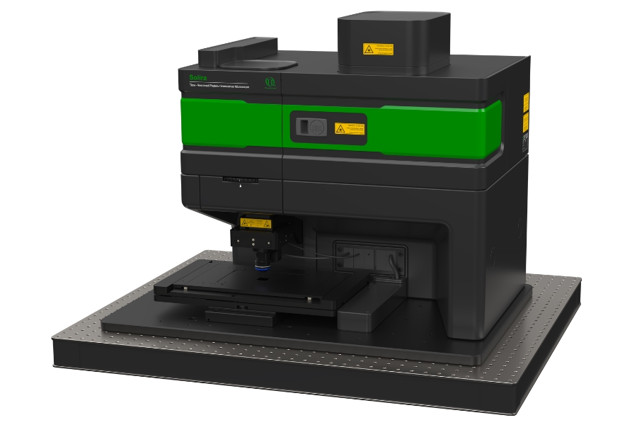
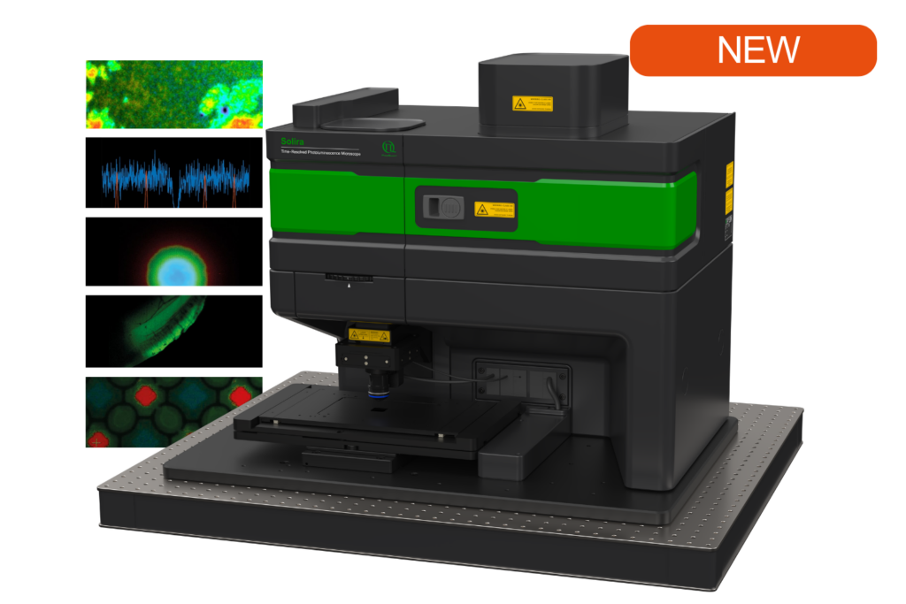
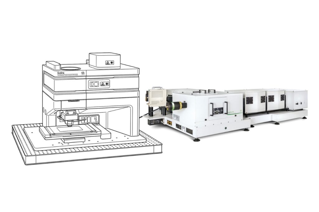
Simplify your materials characterization with one flexible TRPL microscope enabling multiple methods for precise and efficient analysis.
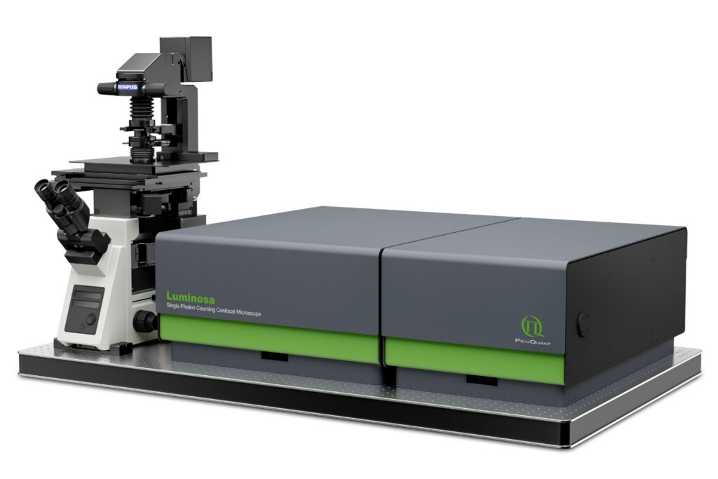
Complete confocal fluorescence microscope that empowers researchers to advance quantitative functional imaging from individual molecules to cells and tissues.
Compact FLIM and FCS upgrade kit that adds advanced functional imaging and correlation analysis to existing laser scanning microscopes.
Designed for flexible, sensitive, and precise steady-state and time-resolved spectroscopy across the UV to NIR range and time scales from picoseconds to milliseconds.
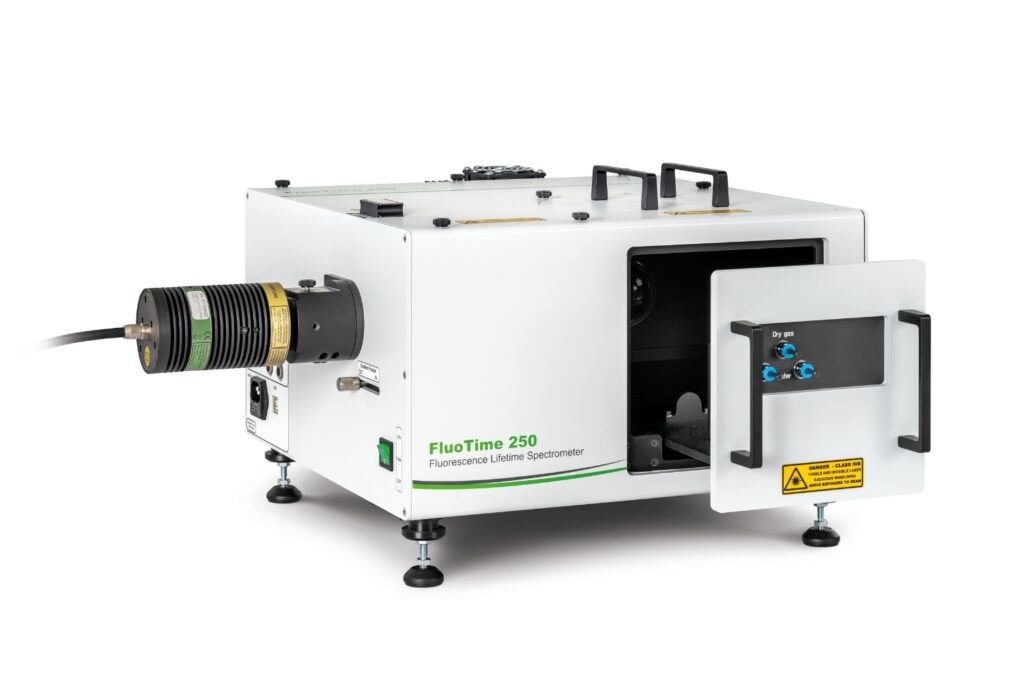
Modular lifetime spectrometer designed for flexible fluorescence and photoluminescence measurements in both materials and life science research.
Add spectral and time-resolved photoluminescence to your setup through flexible microscope–spectrometer coupling options.
Get the most out of superconducting nanowire detectors in large-scale quantum communication and computing experiments requiring precise multichannel timing.
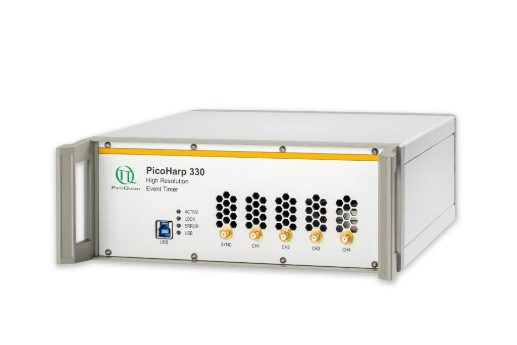
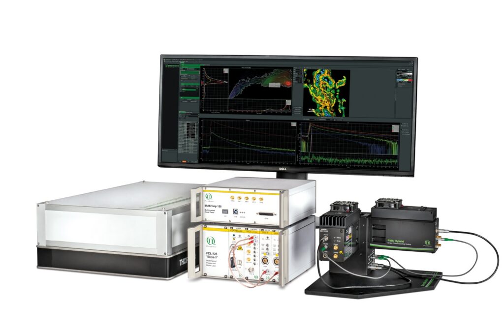
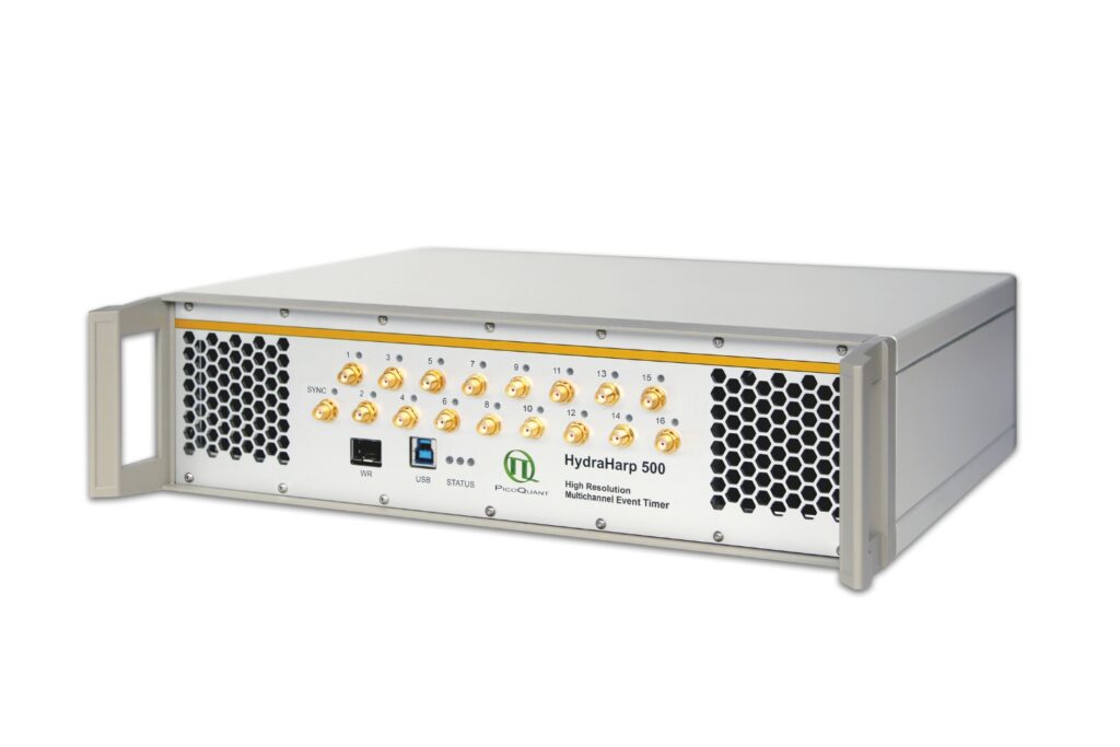
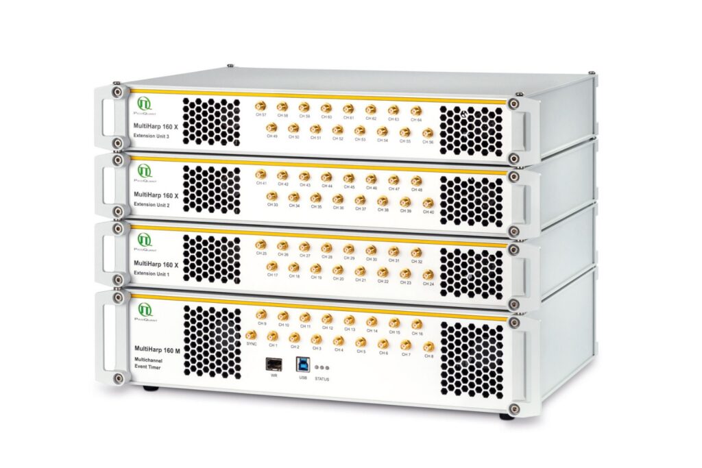
Boost your time-resolved experiments with a flexible, high-precision time tagging and TCSPC unit for materials science and quantum sensing.
Scale your photonic quantum computing and detector characterization setups while maintaining performance, flexibility, and high data throughput.
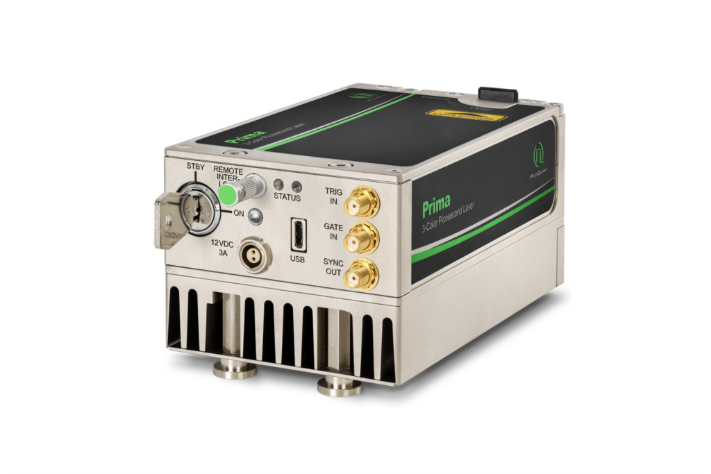
Compact 3-color picosecond laser delivering flexible ns to ms excitation with cost-effective multicolor performance and straightforward operation.
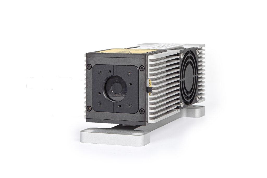
Smart picosecond laser diode heads covering UV-A to NIR, providing the right combination of power, pulse width, and diode type for any time-resolved technique.
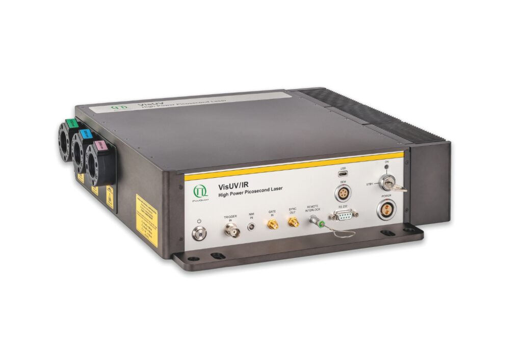
VisUV provides clean short pulses and stable timing across key UV and visible wavelengths, including deep UV lines as well as 488 nm and 532 nm.
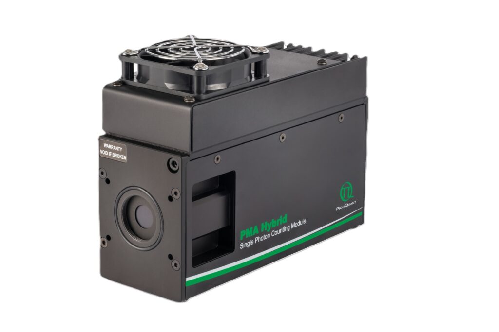
Enhance your single-photon counting experiments with wide dynamic range and excellent timing precision in the UV and visible even at the highest count rates.
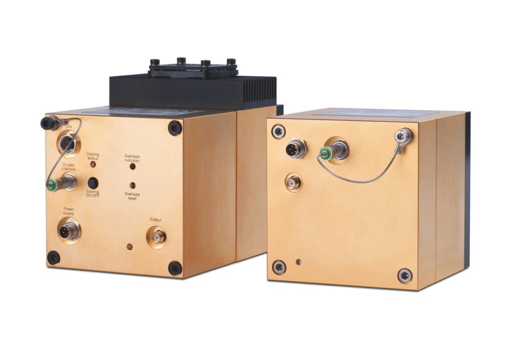
Capture even the weakest signals over large areas with maximum dynamic range and enhanced low-light sensitivity in a compact detector design.
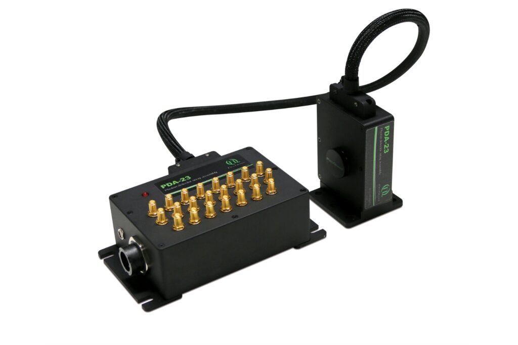
Unlock spatially resolved single-photon detection with a 23-pixel SPAD array, combining low dark counts and precise time tagging for advanced experiments.
Advanced FLIM analysis software for fast, accurate interpretation of lifetime imaging data.
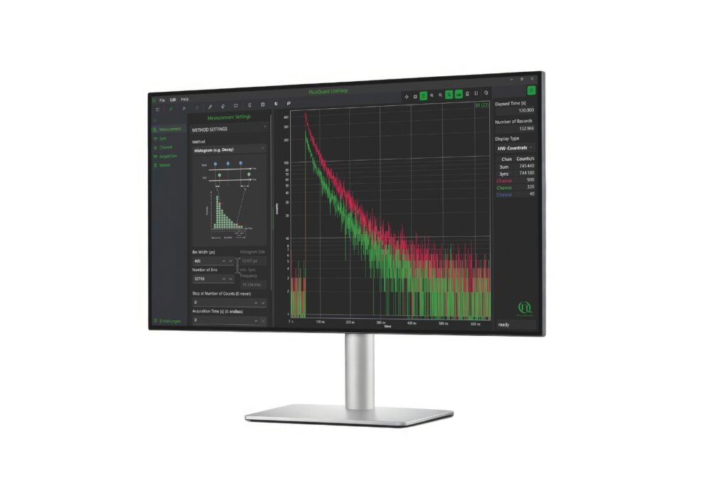
Intuitive, free software solution for real-time, high-precision photon data acquisition, visualization, and initial data analysis.
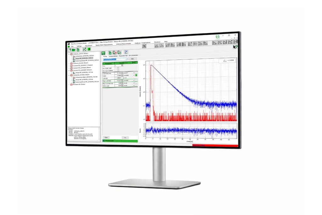
Advanced software for time-resolved fluorescence acquisition and analysis.
An imaging technique that uses fluorescence lifetimes to generate image contrast.
Investigating how proteins dynamically explore multiple conformational states that control biological function.
Investigating how biomolecules separate into dynamic liquid phases to organize cellular space and regulate biological function.
A time-resolved technique that measures photoluminescence lifetimes to reveal excited-state dynamics in materials.
Studying exciton dynamics, charge carrier processes, and structural properties through optical and time-resolved characterization methods.

Investigating charge-carrier lifetimes and recombination dynamics to enable precise optical characterization of material quality and device performance.

A quantum optical signature revealed by time-resolved photon correlation analysis to identify single-photon emission in materials and nanostructures.
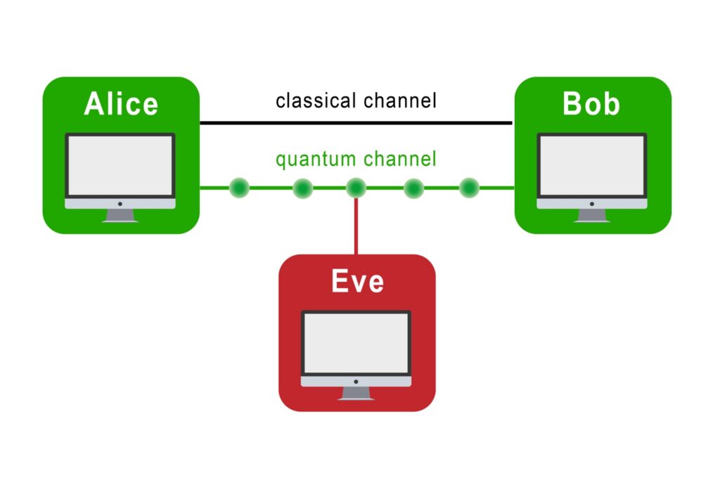
The transmission of information using individual photons, using quantum effects to ensure absolute security.
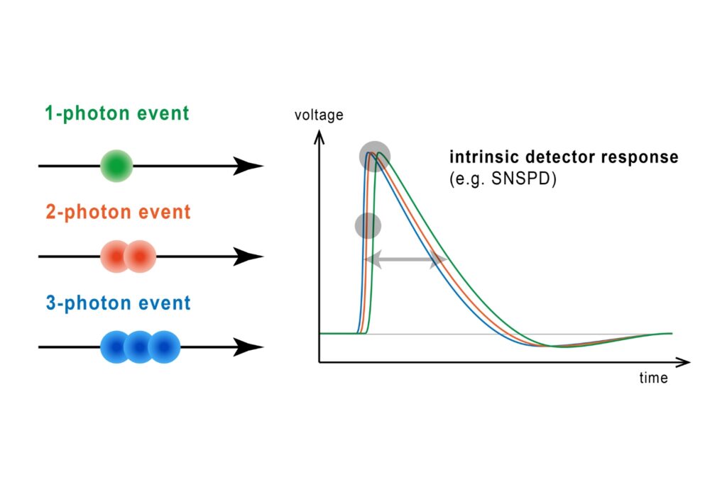
Quantifying photons per detection event enables direct access to photon-number statistics, providing insight into quantum and statistical properties of light.
An optical technique that analyzes light emission under electrical excitation to reveal electronic properties of electroluminescent materials.
Monitoring environmental signals and trace compounds to understand dynamic changes in natural and engineered environments.
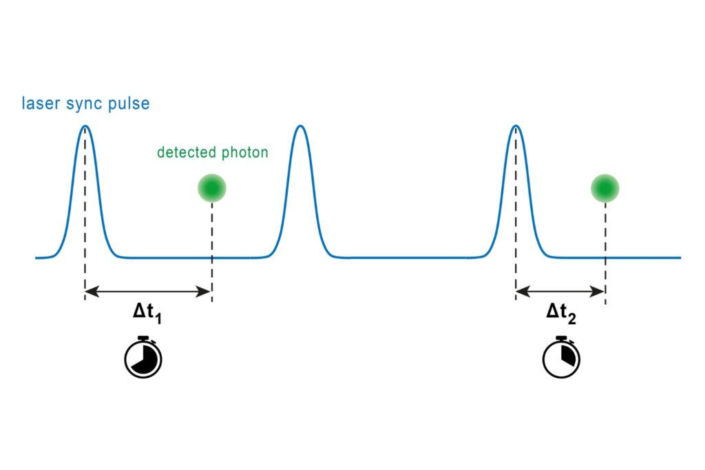
A photon timing technique that measures single-photon arrival times to resolve ultrafast dynamics in fluorescence, materials research, and quantum optics.
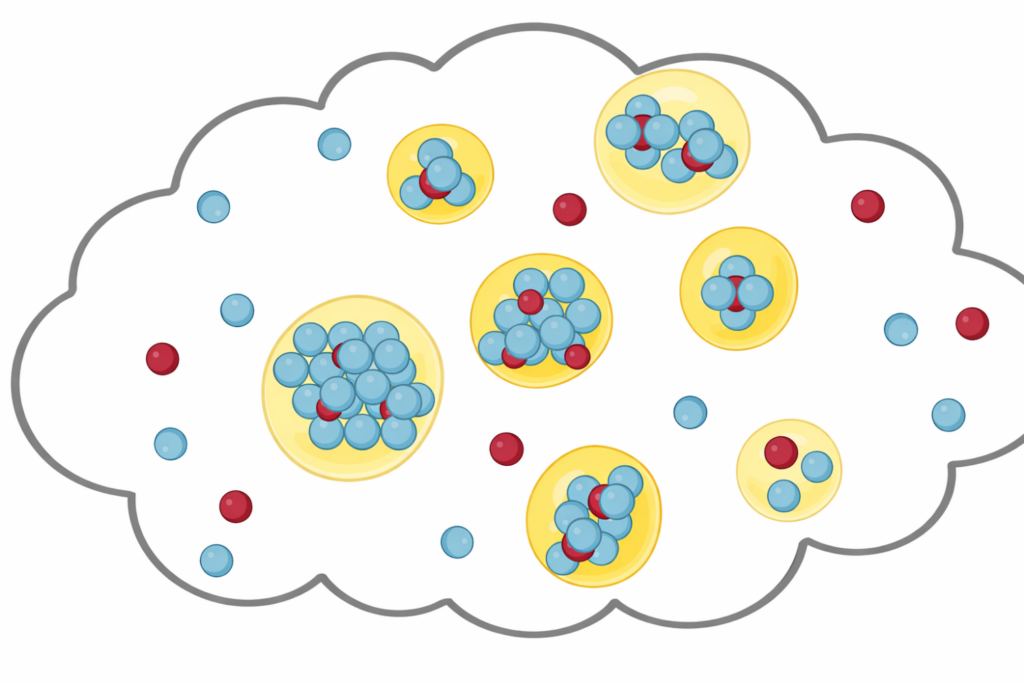
Semiconductors are materials whose electrical and optical properties can be precisely tuned by controlling their composition, structure, and dimensionality. Semiconductor research seeks to understand how these parameters determine charge generation, transport, and recombination. In materials science, this research goes beyond device performance and targets fundamental photophysical processes within the material. Optical characterization techniques play a central role by enabling non contact access to intrinsic properties across different semiconductor classes, including compound semiconductors and quantum well structures.
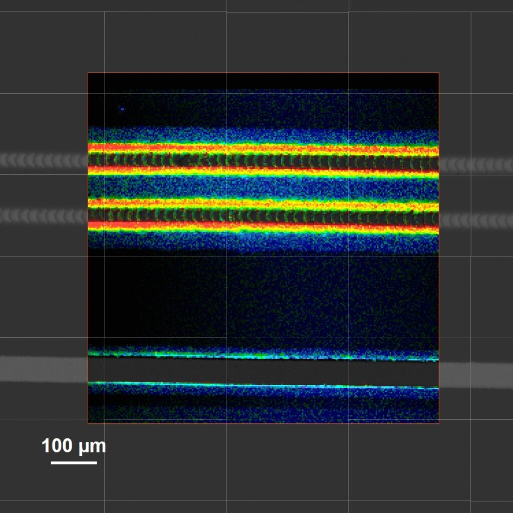
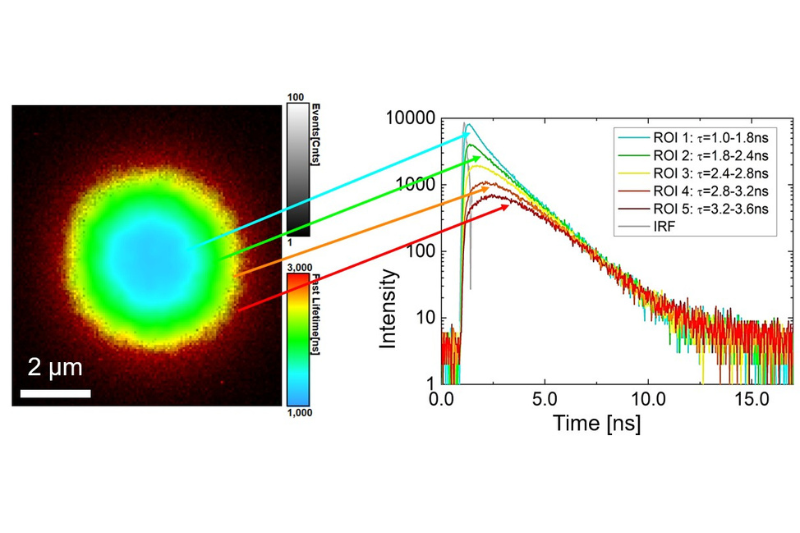
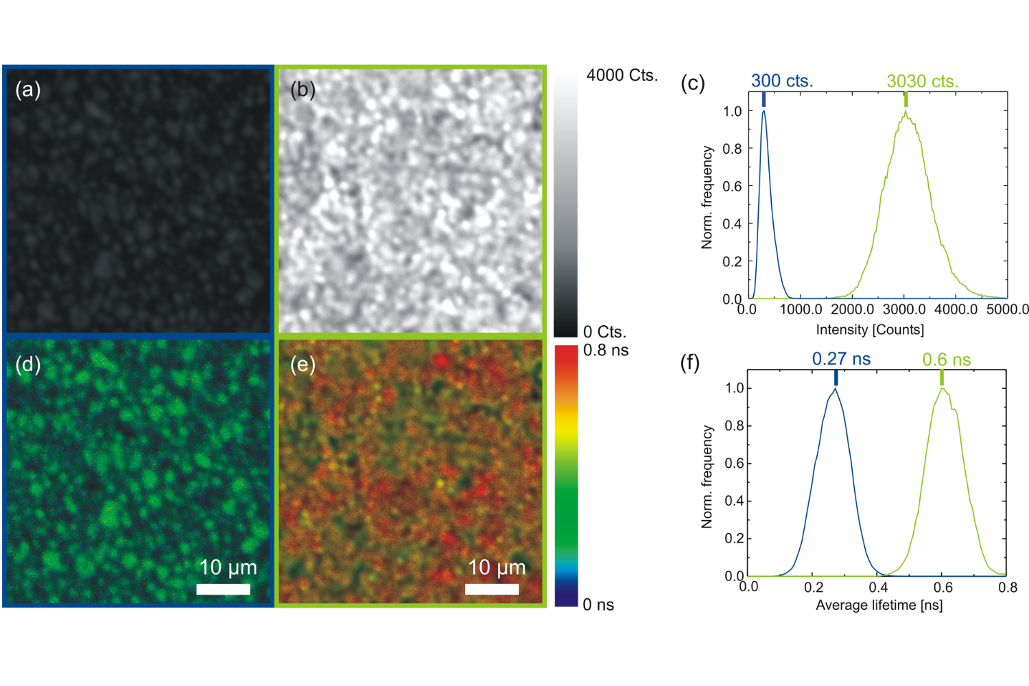
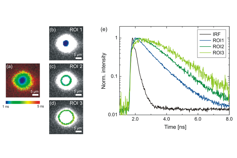 TRPL image following localized excitation at the center of the sample. Middle: Regions of interest with increasing distance from the excitation spot. Right: Normalized photoluminescence decay curves extracted from each region of interest, showing increasing average lifetimes due to carrier diffusion before recombination.
Charge carrier dynamics determine how efficiently a semiconductor absorbs light, transports charge, and converts energy. Carrier lifetimes, recombination pathways, and diffusion processes are directly linked to defects, interfaces, and material quality. Studying these dynamics provides critical insight into loss mechanisms and performance limits of optoelectronic materials, making them a key focus of semiconductor research at the materials level.
Photoluminescence reveals a range of photophysical processes that govern semiconductor behavior. These include radiative and non radiative recombination, carrier trapping, diffusion, and spatial inhomogeneities across a sample. Variations in emission lifetime and intensity reflect changes in material quality, defect density, and local structure, making their study essential for linking microscopic properties to macroscopic optoelectronic performance.
Probing these processes is essential for linking microscopic properties to macroscopic optoelectronic performance.
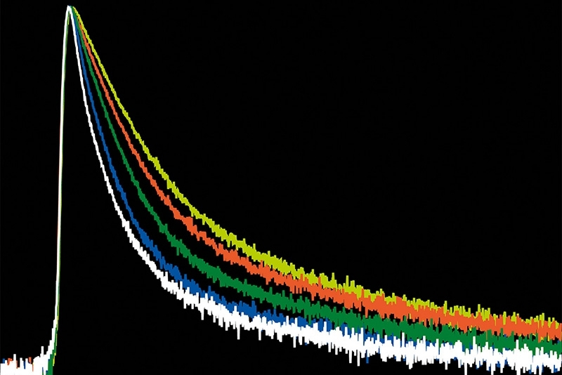
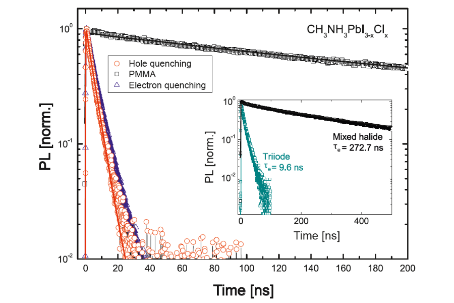 Measured photoluminescence decay curves from mixed halide (inset, black) and triiodide (inset, turquoise) perovskite layers, as well as of the mixed halide material in presence of electron (blue) or hole (red) quenching layer, or PMMA coating (black). The measured decay can be fitted to diffusion models, allowing determining the electron-hole diffusion.
Photoluminescence methods provide direct optical access to charge carrier dynamics in semiconductor materials. Steady state measurements probe emission properties, while time resolved techniques quantify carrier lifetimes and recombination kinetics. Spatially resolved approaches, such as time-resolved photoluminescence (TRPL) imaging, extend this analysis by mapping local variations across complex structures. These techniques enable quantitative, non-contact characterization of optoelectronic materials.
The following application examples show how photoluminescence-based techniques are used to investigate charge carrier dynamics in semiconductor materials. Spectral, temporal, and spatially resolved measurements provide access to recombination, diffusion, and layer-specific processes in complex semiconductor structures.
High spatial resolution TRPL microscopy enables non destructive investigation of charge carrier dynamics in semiconductor materials and quantum well structures. The poster summarizes carrier diffusion imaging, power dependent TRPL, and spectrally resolved measurements, illustrating how spatial and temporal photoluminescence analysis reveals structure to photophysics relationships in complex semiconductor systems.
Time-resolved fluorescence spectroscopy and microscopy provide quantitative access to excited-state and charge carrier dynamics in semiconductor materials. This application note summarizes lifetime-based methods such as TRPL, FLIM, and correlation spectroscopy, demonstrating how temporal and spatial resolution reveal recombination, diffusion, and mobility-related processes beyond steady-state measurements.
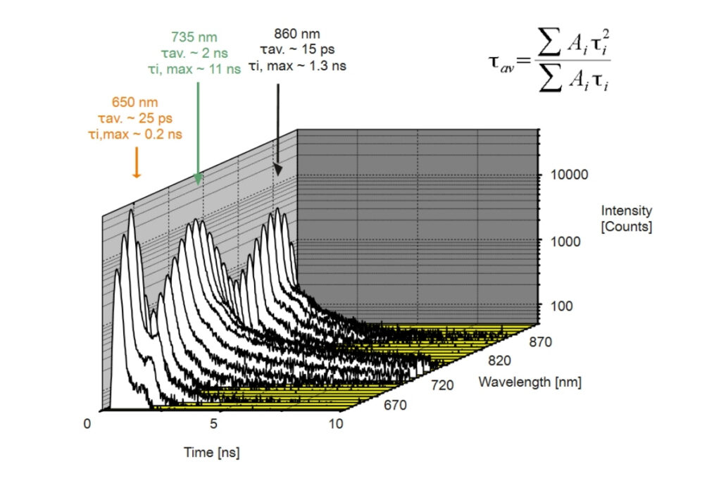
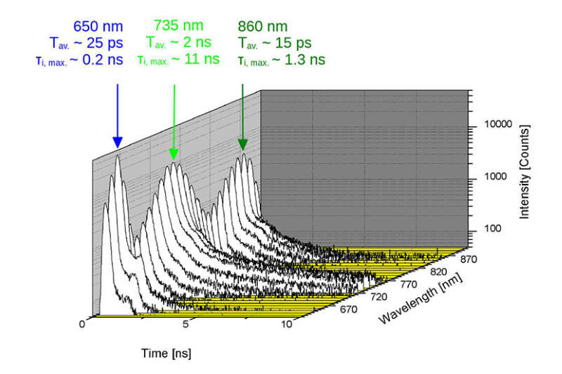
Time-resolved emission spectra (TRES) were used to separate charge carrier dynamics in a GaAsP quantum well heterostructure. Emission peaks at 650 nm, 735 nm, and 860 nm are assigned to the Al₀.₄Ga₀.₆As barrier, the GaAsP quantum well, and the n-GaAs layer and the GaAs substrate. Layer-specific lifetimes reveal distinct recombination dynamics within the multilayer system.
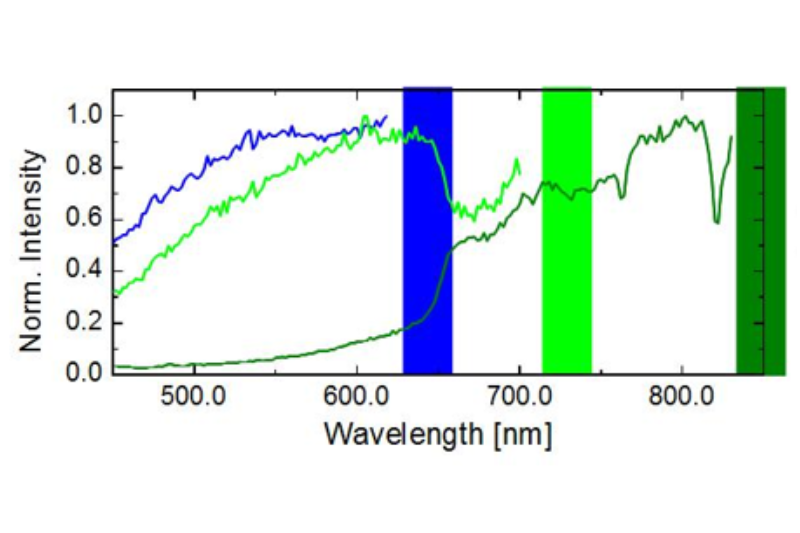
Excitation spectra were recorded for three emission channels of a quantum well wafer: 650 nm (Al₀.₄Ga₀.₆As barrier, blue), 735 nm (GaAsP quantum well, light green), and 860 nm (n-GaAs layer and GaAs substrate, dark green). A dip around 650 nm in the 735 nm channel indicates barrier–well interaction, while the rise in the 860 nm channel correlates with the absorption edge of the barrier at wavelengths longer than the barrier band gap. Colored bands mark the layer band gaps.
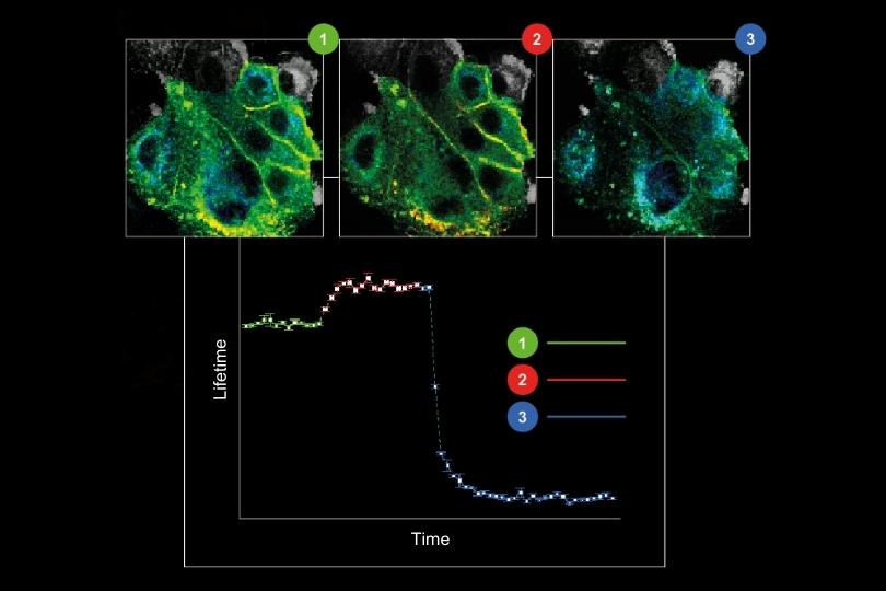
Following localized excitation with a pulsed 440 nm laser, TRPL imaging was used to monitor charge carrier diffusion in a semiconductor sample. Lifetimes extracted from regions of interest (ROI) with increasing distance from the excitation spot increase systematically, reflecting the additional time required for carriers to diffuse before recombination. This spatially resolved delay provides direct access to diffusion-related transport processes.