


Key Highlights
- Spatially resolved hyperspectral imaging reveals strongly confined emission regions associated with V-pit microstructures in red InGaN quantum wells.
- Time-resolved photoluminescence distinguishes bright and dark regions through distinct decay components, providing direct evidence of spatially redistributed hole injection.
- Electric field redistribution along semipolar V-pit sidewalls enables three-dimensional hole transport into planar quantum wells.
- Local carrier dynamics measured on the microscale correlate directly with external quantum efficiency and thermal stability at the device level.
- The combination of confocal microscopy and TCSPC-based lifetime spectroscopy is essential for resolving injection pathways in micro-LED research.
Why Red InGaN Micro-LEDs Remain Efficiency-Limited
Long-wavelength InGaN emitters promise monolithic RGB integration on silicon. Yet achieving efficient red emission remains difficult. High indium incorporation increases strain, promotes defect formation, and complicates carrier transport within multiple quantum wells. In particular, insufficient hole injection and enhanced Shockley–Read–Hall recombination limit external quantum efficiency in red micro-LEDs.
Zheng et al., PhotoniX (2025)1, investigated how V-pit microstructures influence carrier transport and recombination in InGaN red micro-LEDs grown on silicon substrates. Rather than treating V-pits purely as structural defects, the authors combined spatially resolved spectroscopy and numerical modeling to analyze their functional role in hole injection.
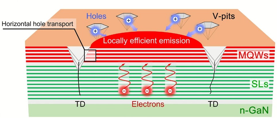
V-Pit Microstructures as Three-Dimensional Injection Pathways
Hexagonal V-pits form around threading dislocations during growth of high-indium InGaN quantum wells. They are typically regarded as structural imperfections associated with nonradiative recombination.
This study shows a more differentiated picture. Rather than acting purely as recombination centers, V-pits can modify the local electric field distribution and create three-dimensional current pathways along their semipolar sidewalls. The inclined quantum wells inside the V-pits differ in thickness and composition from planar wells, which alters band structure and carrier transport.
Understanding whether these microstructures degrade or enhance performance requires spatially resolved and time-resolved optical analysis.
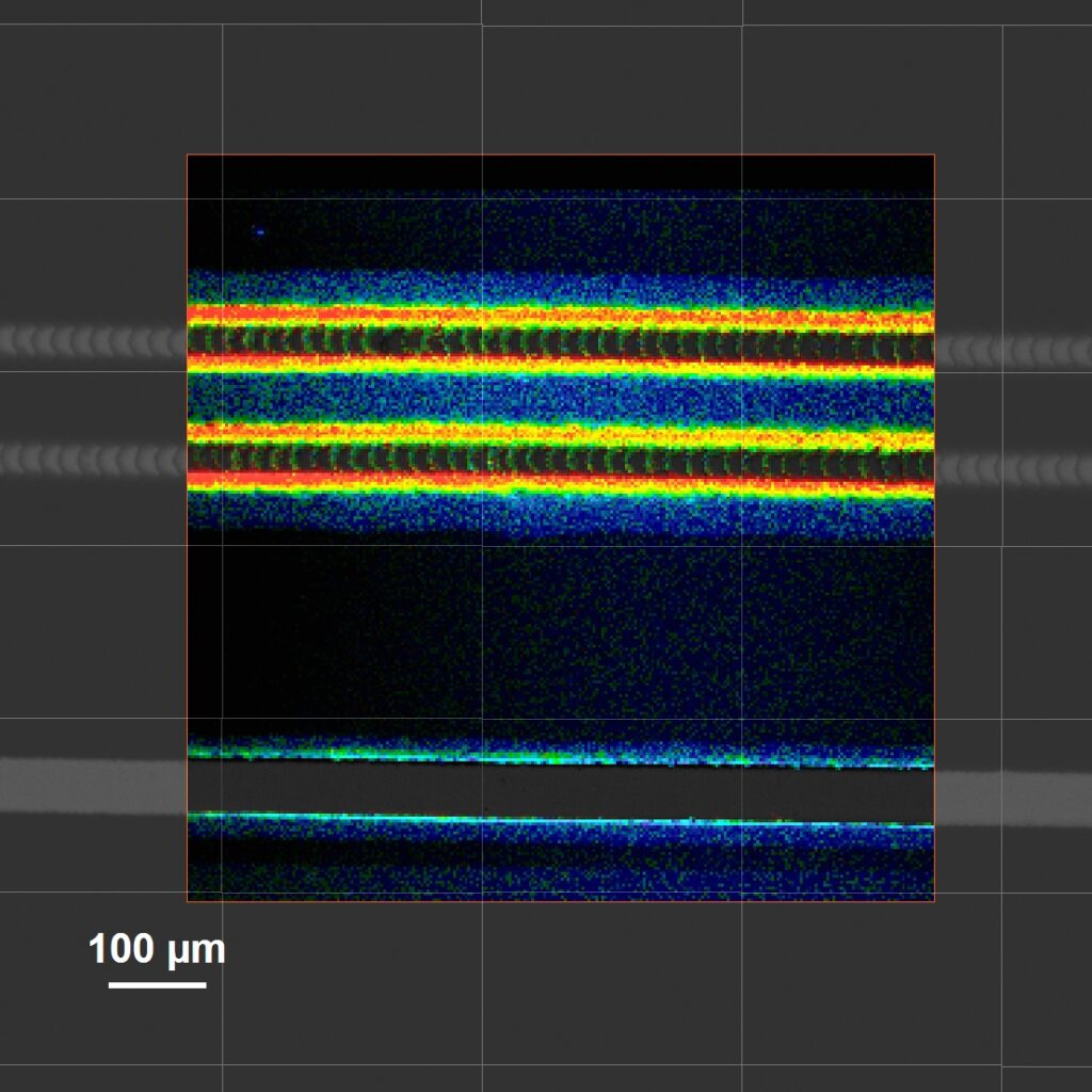
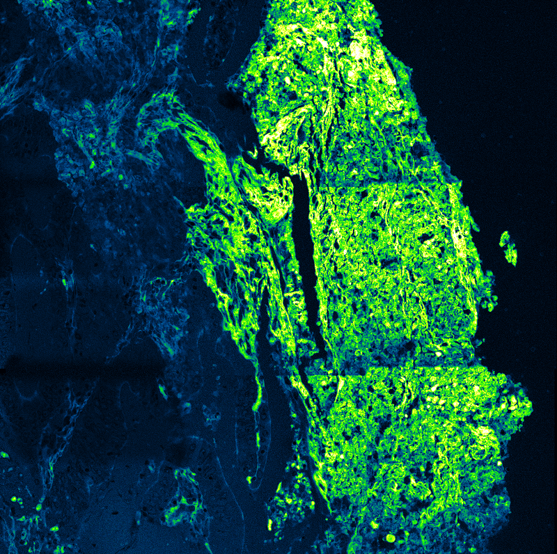
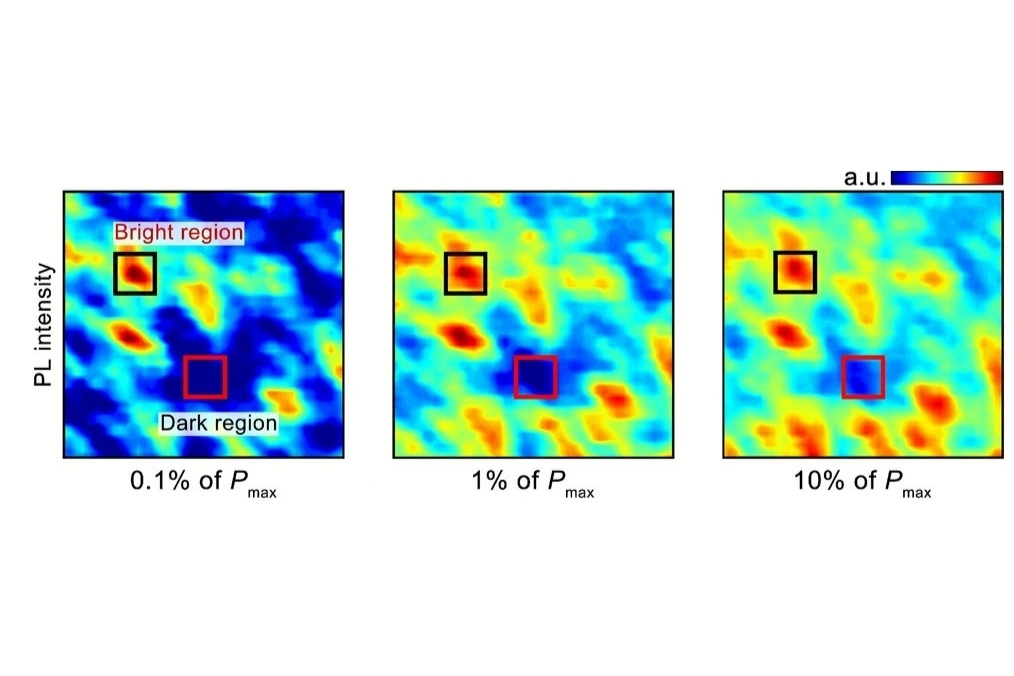
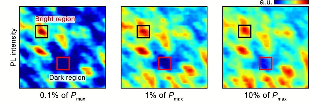
Microscopic Hyperspectral Imaging Reveals Spatially Confined Emission
Confocal micro-photoluminescence mapping reveals discrete bright and dark emission regions within the red InGaN multiple quantum wells. At low excitation densities, emission is strongly localized. With increasing excitation, spatial contrast decreases, but locally enhanced regions remain distinguishable.
Cathodoluminescence and electroluminescence mapping confirm that emission near V-pits differs spectrally and spatially from surrounding planar regions. These observations indicate that carrier confinement and recombination are not uniform across the active region.
Such spatial heterogeneity cannot be captured by area-integrated spectroscopy. Microscopic hyperspectral imaging makes the link between structural features and emission behavior experimentally accessible.
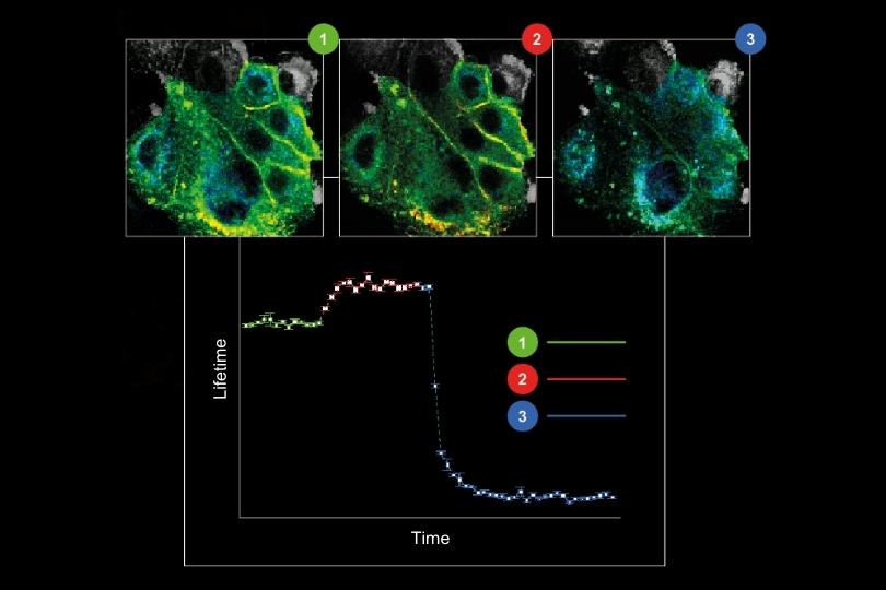
Time-Resolved Photoluminescence Distinguishes Bright and Dark Regions
Time-resolved photoluminescence provides further insight into local carrier dynamics. Bright and dark regions exhibit distinct decay components and transient rise times.
The shorter decay component in darker regions indicates enhanced nonradiative recombination or carrier transfer processes. In contrast, bright regions show longer effective lifetimes consistent with more efficient radiative recombination. Differences in rise time suggest that hole transport from semipolar sidewalls into planar quantum wells contributes to the observed emission patterns.
These lifetime variations provide experimental evidence that carrier injection is spatially redistributed by the V-pit microstructure. Without time-resolved spectroscopy, such injection pathways would remain speculative.
Electric Field Redistribution Explains Local Hole Transport
Numerical simulations support the experimental findings. Calculated band profiles and potential distributions show that the electric field is redirected along the inclined sidewalls of V-pits. This redistribution enables holes to drift from semipolar quantum wells into adjacent planar wells, forming a two-stage injection pathway.
The simulations alone would not establish functional relevance. Their agreement with spatially resolved lifetime and emission data connects electric field redistribution directly to measurable recombination behavior.
V-pits therefore act as geometrically defined injection modifiers rather than passive defects.
From Local Carrier Dynamics to Device-Level Performance
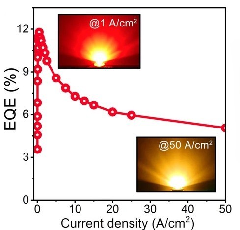
The modified injection pathways correlate with improved device characteristics. The InGaN red LEDs achieve a peak external quantum efficiency of 11.78 percent. Ten-micrometer micro-LEDs fabricated from the same epitaxy reach an on-chip peak EQE of 1.10 percent at 300 K.
Temperature-dependent measurements reveal a characteristic temperature up to 221 K at higher current densities, indicating reduced sensitivity to thermally activated nonradiative recombination. The comparatively small wavelength shift with temperature further supports stable carrier confinement.
These macroscopic metrics reflect microscopic carrier dynamics. Spatially resolved spectroscopy links structural microfeatures to injection efficiency, recombination balance, and ultimately device performance.
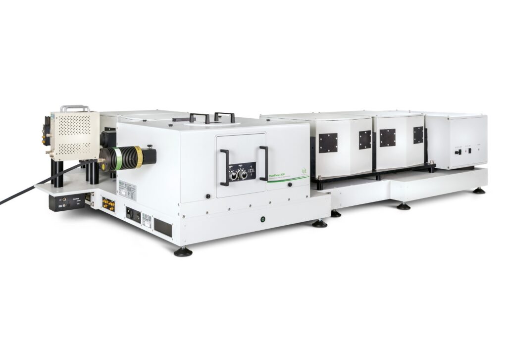
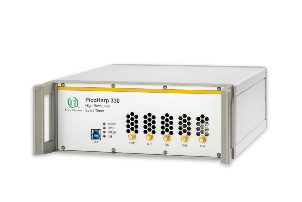
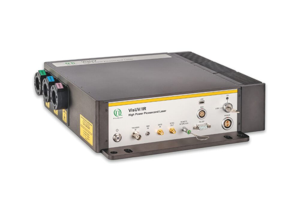
Instrumentation Used in This Study by PicoQuant
This study employed a micro-photoluminescence platform combining the FluoMic widefield photoluminescence microscope with the FluoTime 300 photoluminescence spectrometer.

Key experimental requirements included:
- Spatial resolution on the sub-micrometer scale to resolve individual V-pit regions
- Spectral discrimination of locally confined emission
- Nanosecond-scale lifetime resolution for biexponential decay analysis
- Stable excitation at 405 nm for selective excitation of the quantum wells
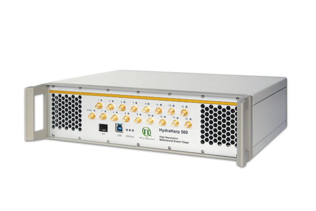
The combination of confocal microscopy and time-resolved single-photon counting enabled direct correlation between microstructure, carrier lifetime, and emission efficiency. Such integration of spatial and temporal resolution is essential for understanding injection mechanisms in micro-LED research.
1 Reference: Xi Zheng, Guobao Zhao, Yurong Dai, Yi Fu, Mingbing Zhou, Tao Huang, Swee Tiam Tan, Vijay Kumar Sharma, Yijun Lu, Tingzhu Wu, Hilmi Volkan Demir, Zhong Chen & Weijie Guo. V-pit-induced electric field redistribution enabling efficient hole injection in InGaN-based red light-emitting diodes grown on silicon. PhotoniX 6, 55 (2025). https://doi.org/10.1186/s43074-025-00214-2