
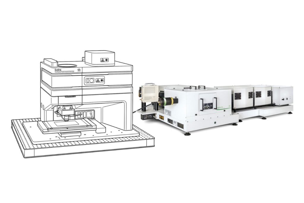
Simplify your materials characterization with one flexible TRPL microscope enabling multiple methods for precise and efficient analysis.
Complete confocal fluorescence microscope that empowers researchers to advance quantitative functional imaging from individual molecules to cells and tissues.
Compact FLIM and FCS upgrade kit that adds advanced functional imaging and correlation analysis to existing laser scanning microscopes.
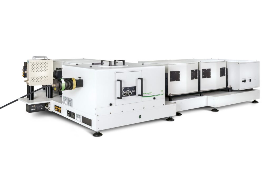
Designed for flexible, sensitive, and precise steady-state and time-resolved spectroscopy across the UV to NIR range and time scales from picoseconds to milliseconds.
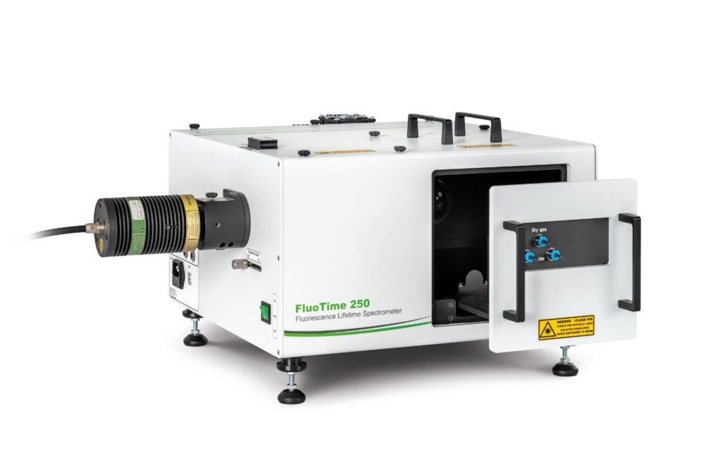
Modular lifetime spectrometer designed for flexible fluorescence and photoluminescence measurements in both materials and life science research.
Add spectral and time-resolved photoluminescence to your setup through flexible microscope–spectrometer coupling options.
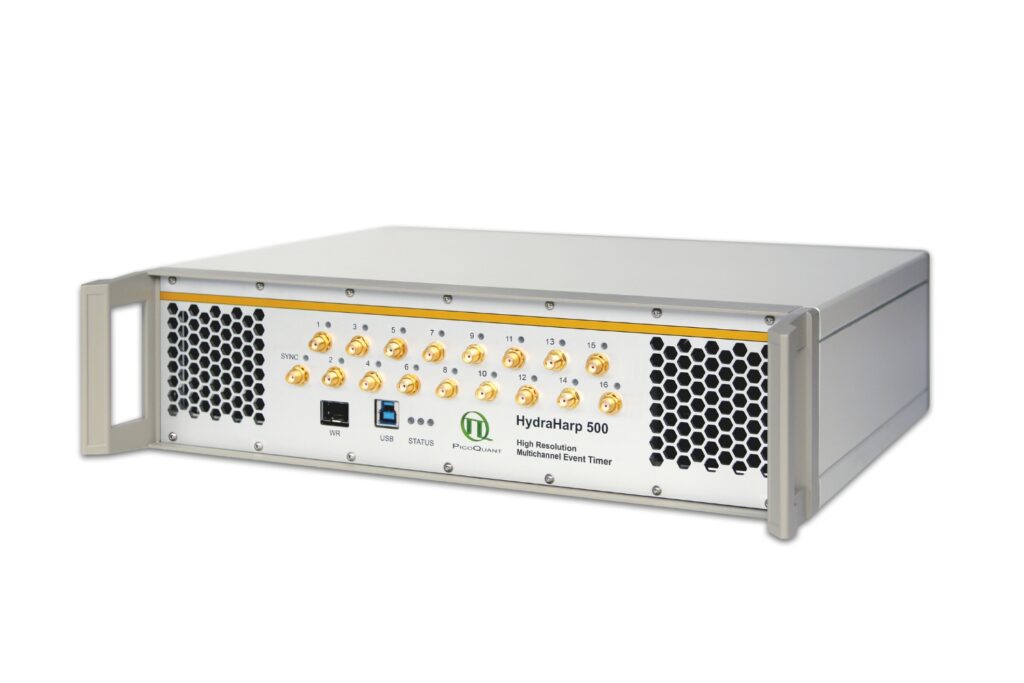
Get the most out of superconducting nanowire detectors in large-scale quantum communication and computing experiments requiring precise multichannel timing.
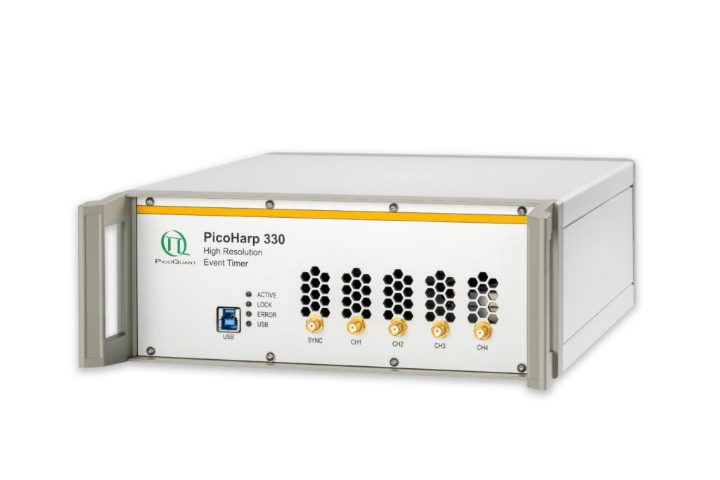
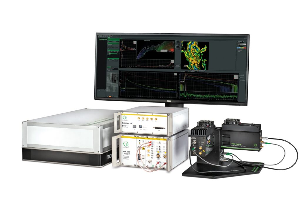
Boost your time-resolved experiments with a flexible, high-precision time tagging and TCSPC unit for materials science and quantum sensing.
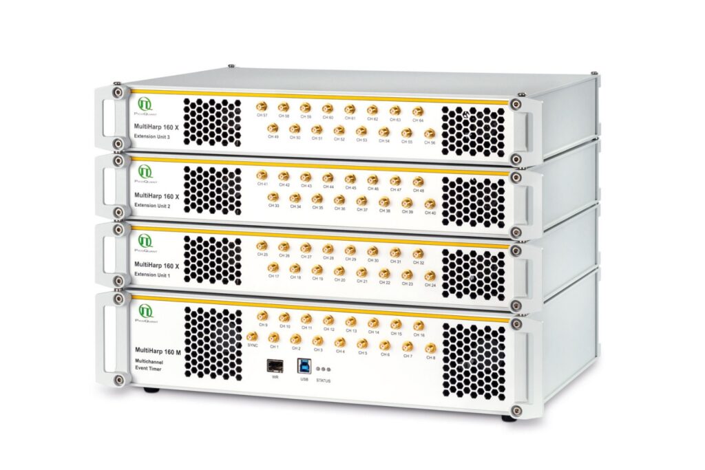
Scale your photonic quantum computing and detector characterization setups while maintaining performance, flexibility, and high data throughput.
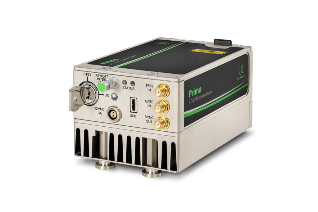
Compact 3-color picosecond laser delivering flexible ns to ms excitation with cost-effective multicolor performance and straightforward operation.
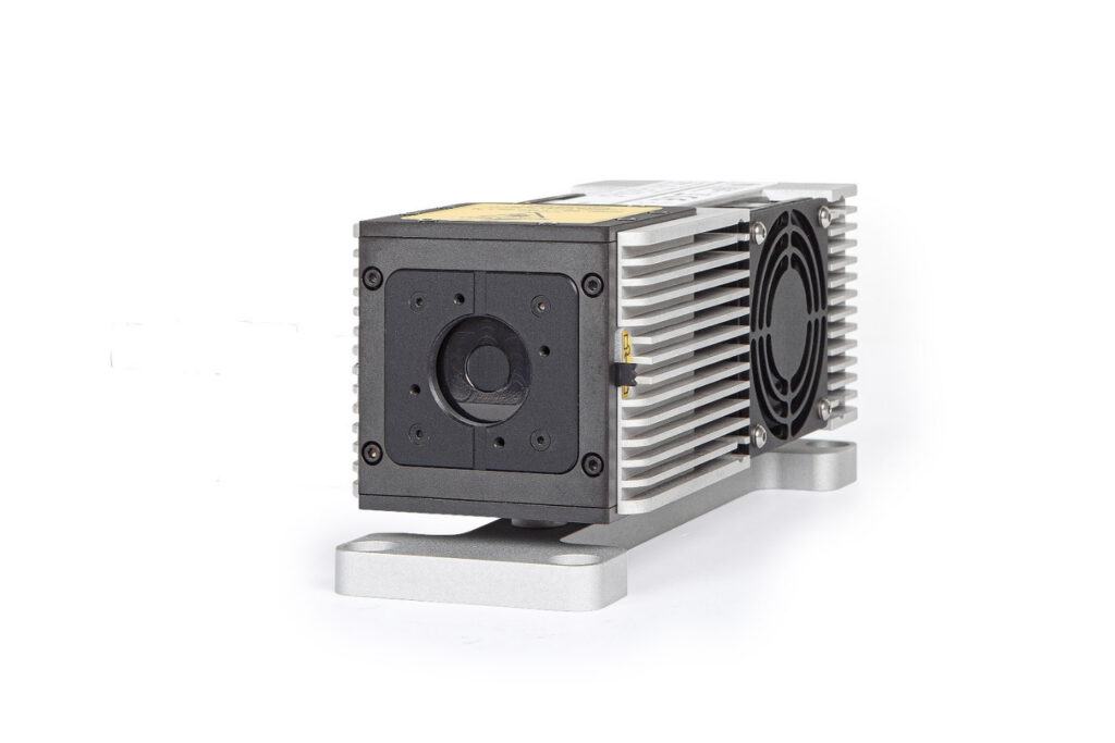
Smart picosecond laser diode heads covering UV-A to NIR, providing the right combination of power, pulse width, and diode type for any time-resolved technique.
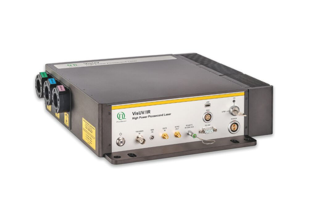
VisUV provides clean short pulses and stable timing across key UV and visible wavelengths, including deep UV lines as well as 488 nm and 532 nm.
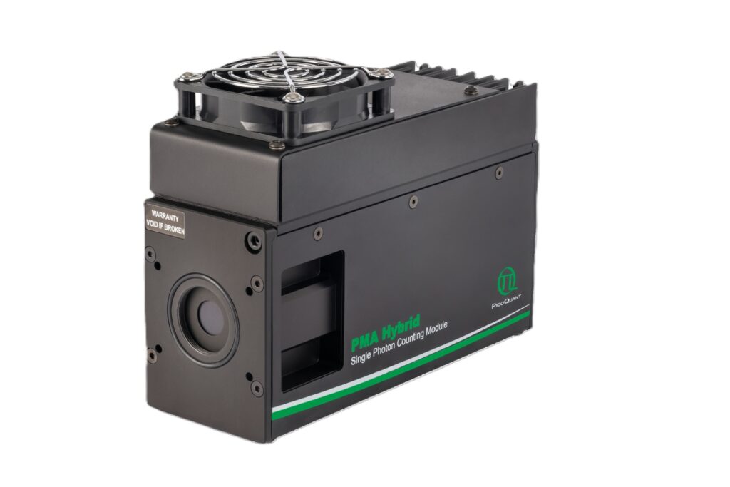
Enhance your single-photon counting experiments with wide dynamic range and excellent timing precision in the UV and visible even at the highest count rates.
Capture even the weakest signals over large areas with maximum dynamic range and enhanced low-light sensitivity in a compact detector design.
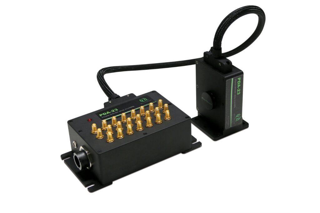
Unlock spatially resolved single-photon detection with a 23-pixel SPAD array, combining low dark counts and precise time tagging for advanced experiments.
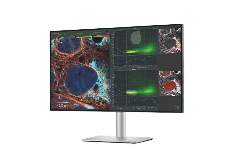
Advanced FLIM analysis software for fast, accurate interpretation of lifetime imaging data.
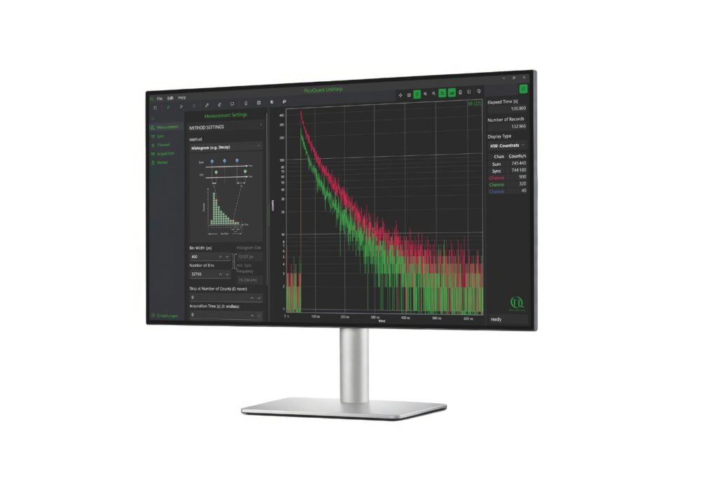
Intuitive, free software solution for real-time, high-precision photon data acquisition, visualization, and initial data analysis.
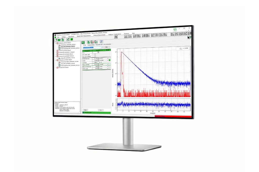
Advanced software for time-resolved fluorescence acquisition and analysis.
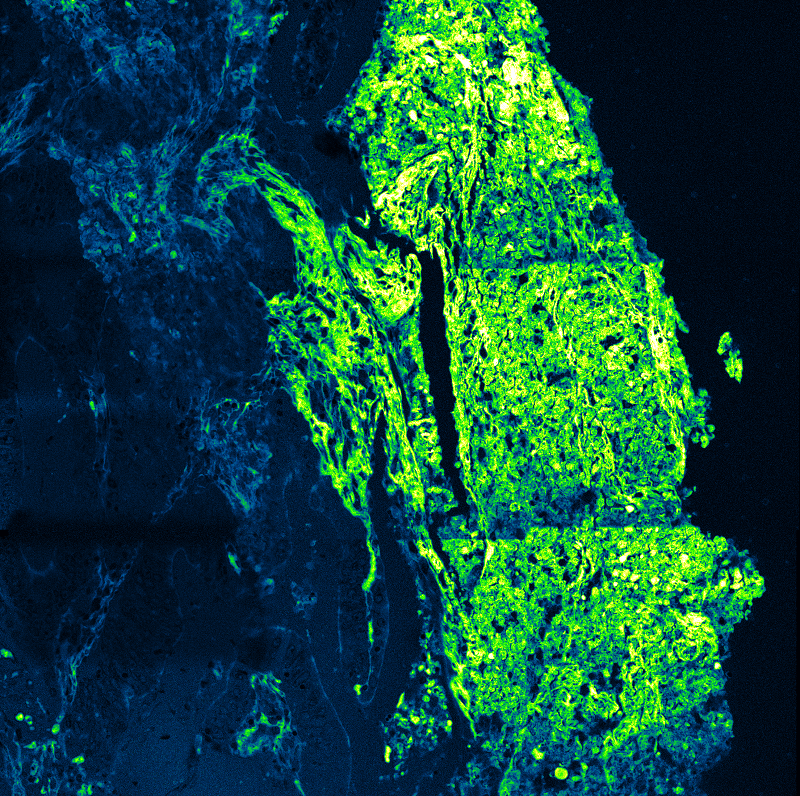
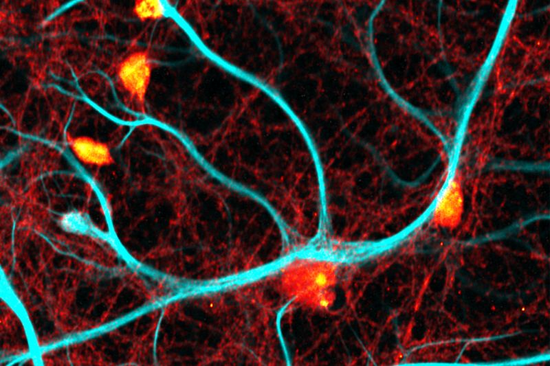
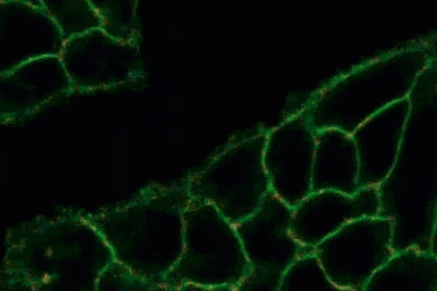
An imaging technique that uses fluorescence lifetimes to generate image contrast.
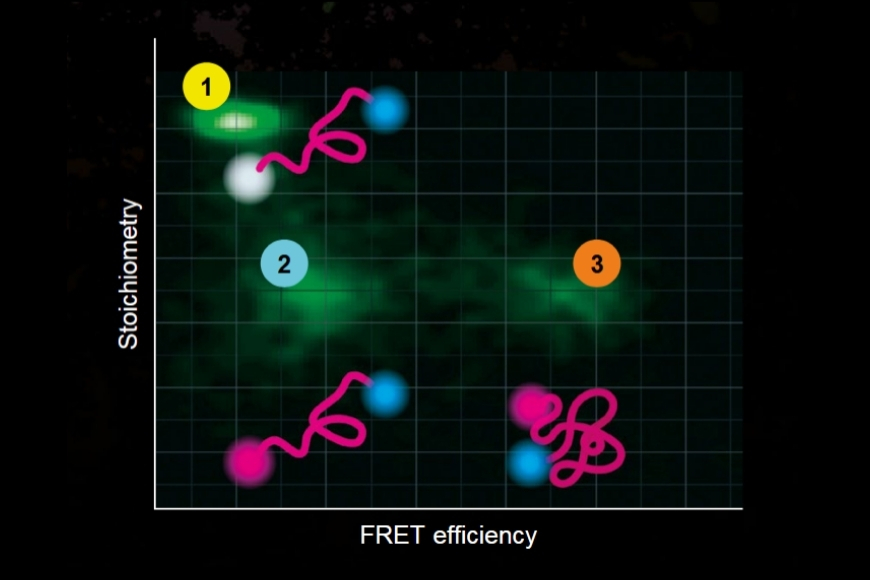
Investigating how proteins dynamically explore multiple conformational states that control biological function.
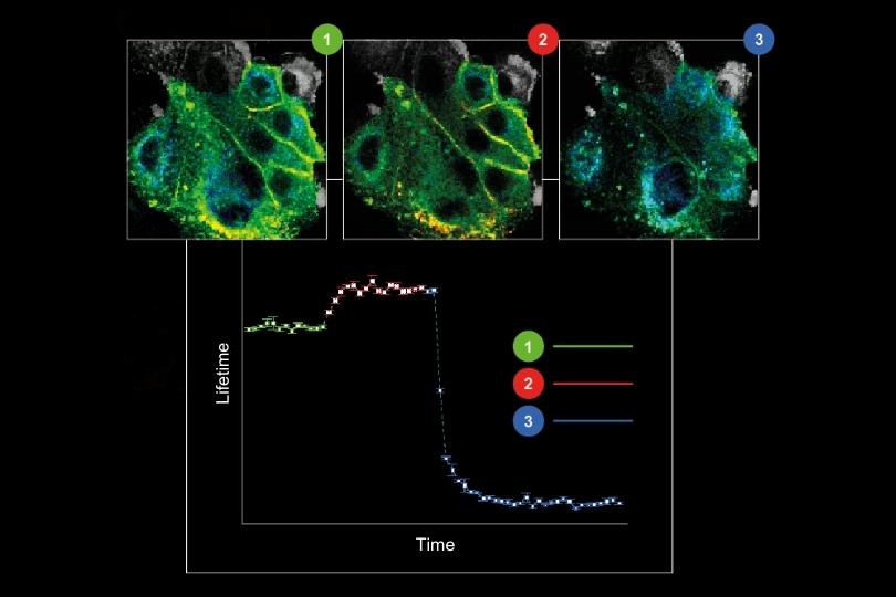
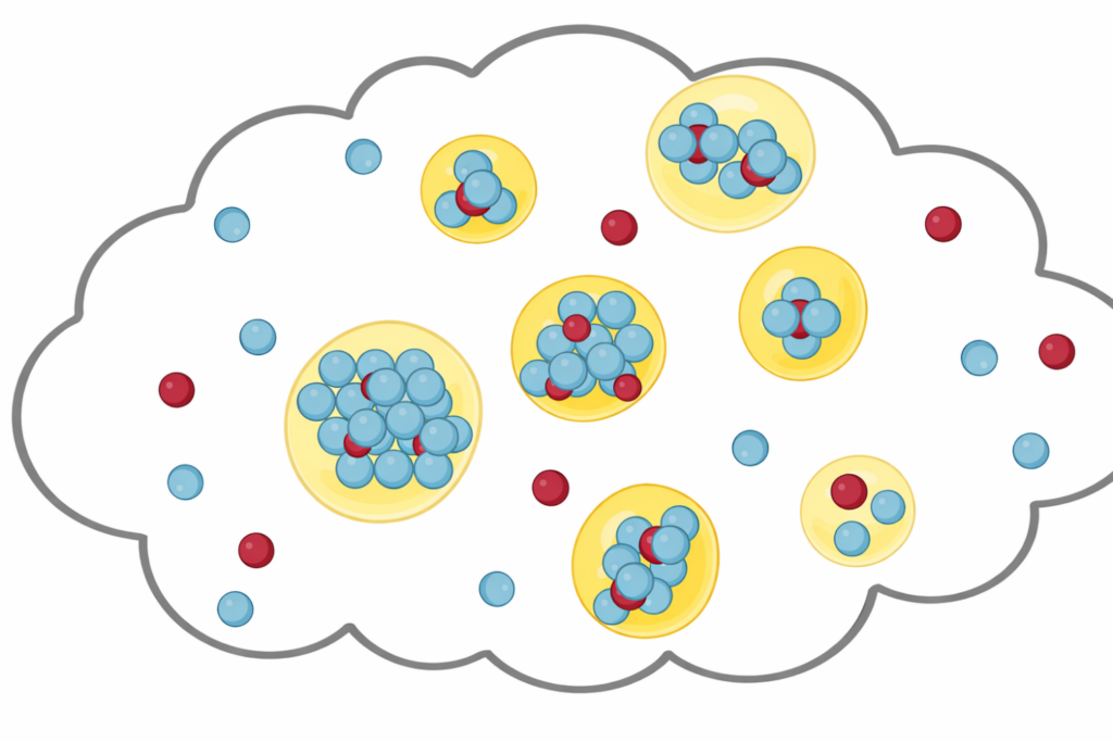
Investigating how biomolecules separate into dynamic liquid phases to organize cellular space and regulate biological function.
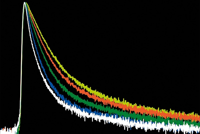
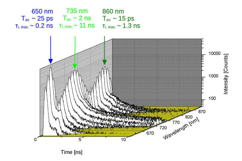
A time-resolved technique that measures photoluminescence lifetimes to reveal excited-state dynamics in materials.
Studying exciton dynamics, charge carrier processes, and structural properties through optical and time-resolved characterization methods.
Investigating charge-carrier lifetimes and recombination dynamics to enable precise optical characterization of material quality and device performance.

A quantum optical signature revealed by time-resolved photon correlation analysis to identify single-photon emission in materials and nanostructures.
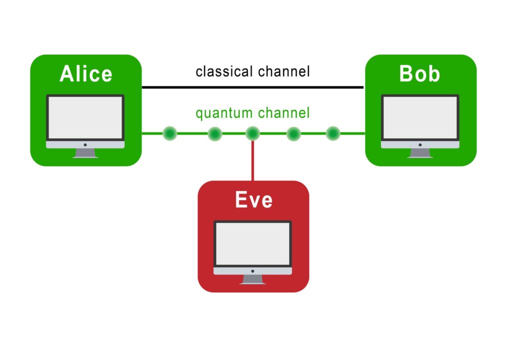
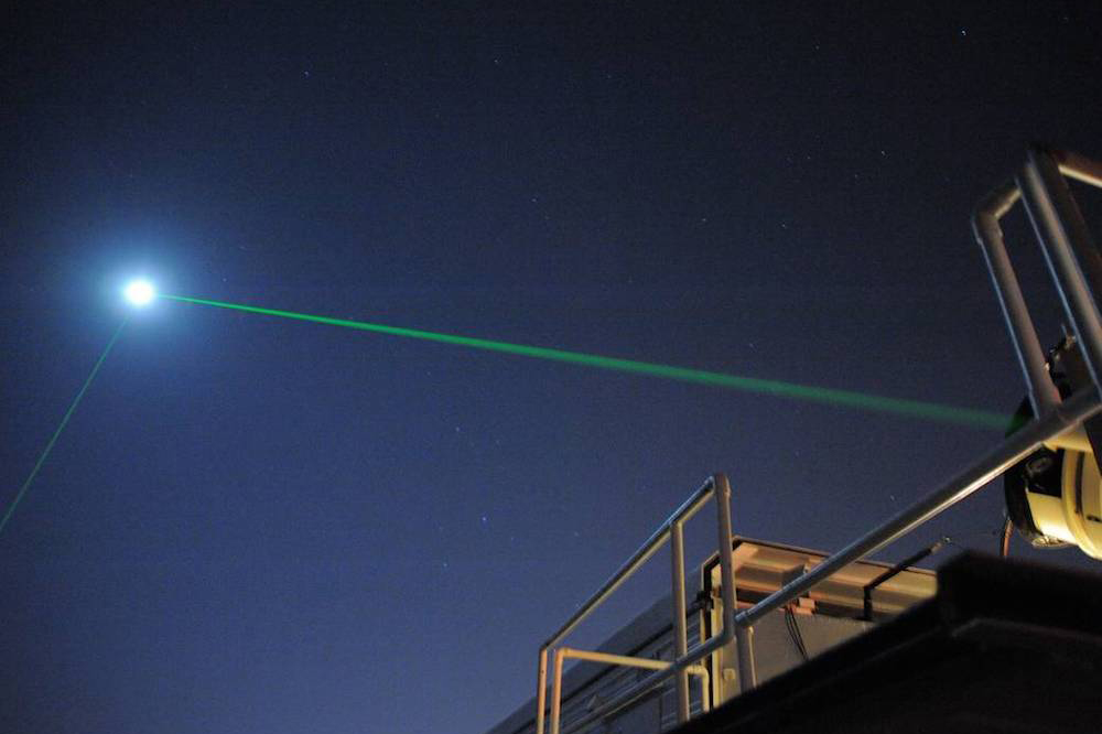
The transmission of information using individual photons, using quantum effects to ensure absolute security.
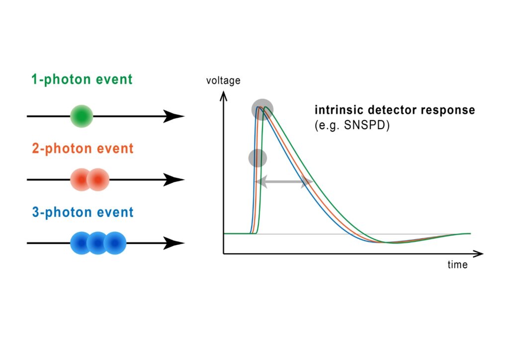
Quantifying photons per detection event enables direct access to photon-number statistics, providing insight into quantum and statistical properties of light.
An optical technique that analyzes light emission under electrical excitation to reveal electronic properties of electroluminescent materials.
Monitoring environmental signals and trace compounds to understand dynamic changes in natural and engineered environments.
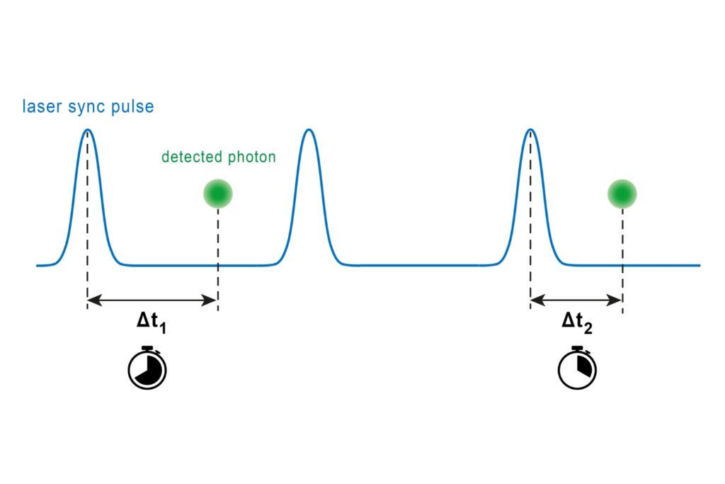
A photon timing technique that measures single-photon arrival times to resolve ultrafast dynamics in fluorescence, materials research, and quantum optics.